The Russian Federal Nuclear Center – VNIIEF, part of the Russian state nuclear corporation Rosatom and known for developing the USSR's first atomic and hydrogen bombs, will develop new equipment for the domestic semiconductor industry.
Tech.az reports that, according to CNews, the Russian Ministry of Industry and Trade (Minpromtorg) has allocated 992.85 million rubles (approximately 12.7 million US dollars) for the implementation of the project.
VNIIEF was the only participant in the competition and signed a contract for the scientific research and experimental design work "Dentist" on July 6, 2026. The project is scheduled to be completed by October 30, 2029.
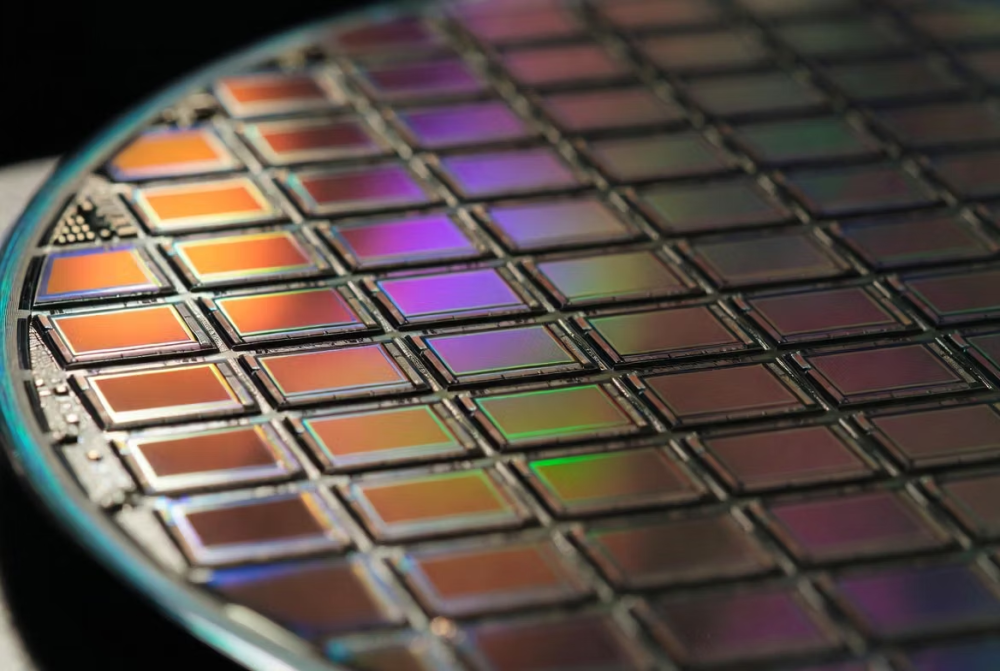
Two main pieces of equipment used in the production of microchips will be developed within the framework of the project. One of them is intended for temporary bonding of silicon wafers with a diameter of 100, 150 and 200 mm (bonding), and the other for their separation and cleaning (debonding).
Temporary bonding technology is widely used in the production of complex microchips. During this process, a silicon wafer is temporarily attached to a special carrier board so that subsequent processing, thinning and transportation stages can be carried out safely. After production is completed, the wafers are separated and adhesive residues are removed using a special debonding system.
According to the technical specifications, the equipment to be manufactured must use domestic components to the maximum extent possible. This includes controllers based on Russian-made processors, domestic microcontrollers and programmable logic circuits (FPGA), vacuum systems, automatic loading-unloading mechanisms and software.
This project is considered part of Russia's strategy to reduce its dependence on foreign technologies and develop microelectronics production in the country.